Contactless Level Measurement of Solids

So far, EBE sensors + motion’s product range of level sensors has covered the detection of liquids with various consistencies. Now, a new technology based on the 2D ToF sensor system extends the portfolio allowing for the contactless level measurement of solids with a great variety of geometries.
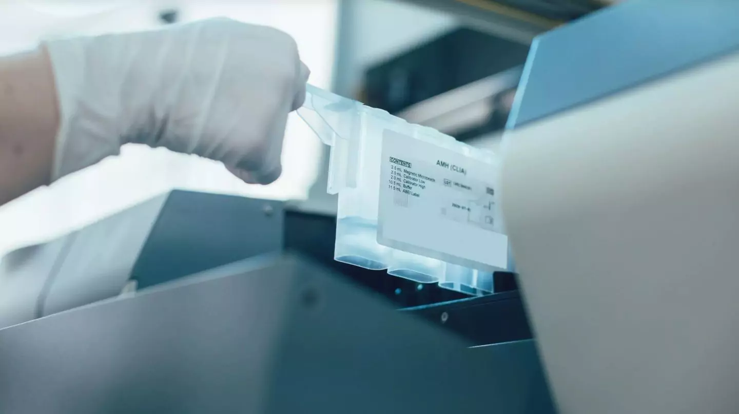
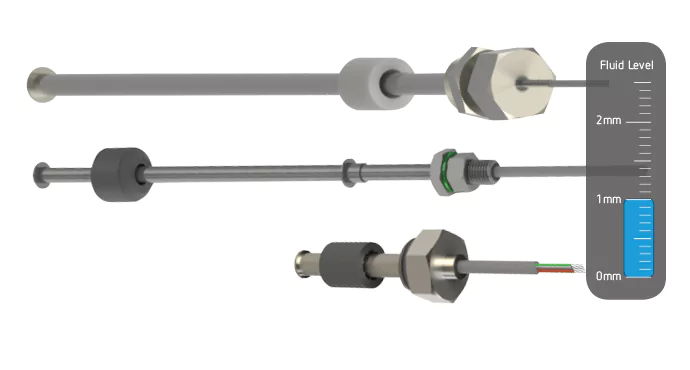
One of the core competencies of EBE sensors + motion is the measurement of liquids without the need to establish direct contact with the medium. In doing so, sensors based on the corTEC© and capaTEC© technologies have proven themselves in a variety of industries. EBE now extends its portfolio by a sensor system based on the 2D ToF technology, thus also offering the contactless level measurement of solids. With this technology, a great variety of media with all kinds of surfaces can be monitored and measured. No matter whether bulk materials or solids such as containers with screws, salt tablets of desalination plants or ice cubes in storage tanks; the sensor system reliably detects the media and provides reliable measurement values of the fill level.
Measurement of Media with Complex Geometries
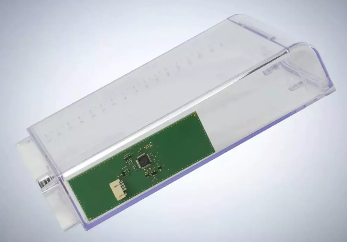
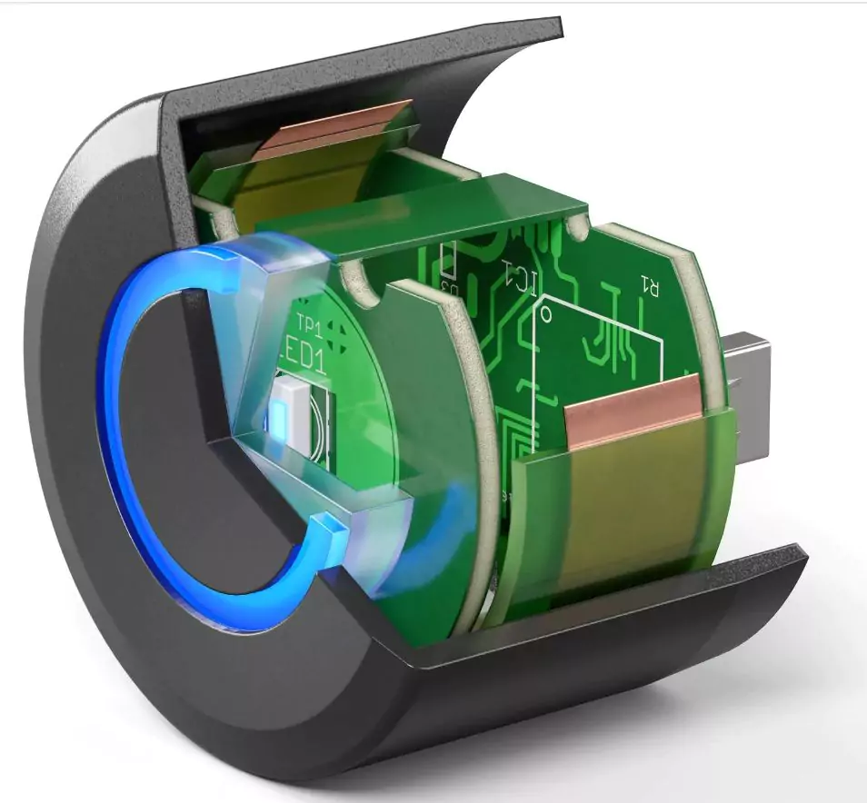
The sensor used is based on an infrared laser and a photodiode reception matrix. The latter emits a laser beam to an object and absorbs the reflected scattered light by means of photocells. Based on the runtime measured, the distance of each object is defined. In this way, even media with extremely complex geometries at the surface can be measured.
Flexible Uses Adapted to Customer Applications
The sensor system can be applied across different distances, from a few centimeters up to 10 meters. The sensors detect fill levels contactlessly through small optical windows, thus offering optimum measurement results for the respective customer applications. They are insensitive to optical interference radiation, e.g. caused by sunlight or other sources of light. Possible interfering objects in the optical field can be faded out by the EBE algorithms. Even so, the sensor is very small and can also be integrated into small installation spaces.

your
local specialist
for